What is MEMS Technology?
Micro-Electro-Mechanical Systems, or MEMS, is a technology that in its most general form can be defined as miniaturized mechanical and electro-mechanical elements (i.e., devices and structures) that are made using the techniques of microfabrication. The critical physical dimensions of MEMS devices can vary from well below one micron on the lower end of the dimensional spectrum, all the way to several millimeters. Likewise, the types of MEMS devices can vary from relatively simple structures having no moving elements, to extremely complex electromechanical systems with multiple moving elements under the control of integrated microelectronics. The one main criterion of MEMS is that there are at least some elements having some sort of mechanical functionality whether or not these elements can move. The term used to define MEMS varies in different parts of the world. In the United States they are predominantly called MEMS, while in some other parts of the world they are called “Microsystems Technology” or “micromachined devices”.
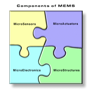
While the functional elements of MEMS are miniaturized structures, sensors, actuators, and microelectronics, the most notable (and perhaps most interesting) elements are the microsensors and microactuators. Microsensors and microactuators are appropriately categorized as “transducers”, which are defined as devices that convert energy from one form to another. In the case of microsensors, the device typically converts a measured mechanical signal into an electrical signal.
Over the past several decades MEMS researchers and developers have demonstrated an extremely large number of microsensors for almost every possible sensing modality including temperature, pressure, inertial forces, chemical species, magnetic fields, radiation, etc. Remarkably, many of these micromachined sensors have demonstrated performances exceeding those of their macroscale counterparts. That is, the micromachined version of, for example, a pressure transducer, usually outperforms a pressure sensor made using the most precise macroscale level machining techniques. Not only is the performance of MEMS devices exceptional, but their method of production leverages the same batch fabrication techniques used in the integrated circuit industry – which can translate into low per-device production costs, as well as many other benefits. Consequently, it is possible to not only achieve stellar device performance, but to do so at a relatively low cost level. Not surprisingly, silicon based discrete microsensors were quickly commercially exploited and the markets for these devices continue to grow at a rapid rate.
More recently, the MEMS research and development community has demonstrated a number of microactuators including: microvalves for control of gas and liquid flows; optical switches and mirrors to redirect or modulate light beams; independently controlled micromirror arrays for displays, microresonators for a number of different applications, micropumps to develop positive fluid pressures, microflaps to modulate airstreams on airfoils, as well as many others. Surprisingly, even though these microactuators are extremely small, they frequently can cause effects at the macroscale level; that is, these tiny actuators can perform mechanical feats far larger than their size would imply. For example, researchers have placed small microactuators on the leading edge of airfoils of an aircraft and have been able to steer the aircraft using only these microminiaturized devices.
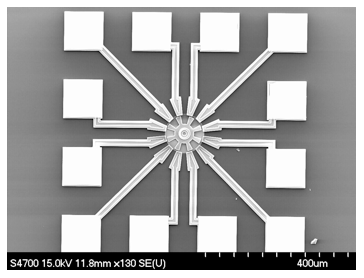
A surface micromachined electro-statically-actuated micromotor fabricated by
the MNX. This device is an example of a MEMS-based microactuator.
The real potential of MEMS starts to become fulfilled when these miniaturized sensors, actuators, and structures can all be merged onto a common silicon substrate along with integrated circuits (i.e., microelectronics). While the electronics are fabricated using integrated circuit (IC) process sequences (e.g., CMOS, Bipolar, or BICMOS processes), the micromechanical components are fabricated using compatible "micromachining" processes that selectively etch away parts of the silicon wafer or add new structural layers to form the mechanical and electromechanical devices. It is even more interesting if MEMS can be merged not only with microelectronics, but with other technologies such as photonics, nanotechnology, etc. This is sometimes called “heterogeneous integration.” Clearly, these technologies are filled with numerous commercial market opportunities.
While more complex levels of integration are the future trend of MEMS technology, the present state-of-the-art is more modest and usually involves a single discrete microsensor, a single discrete microactuator, a single microsensor integrated with electronics, a multiplicity of essentially identical microsensors integrated with electronics, a single microactuator integrated with electronics, or a multiplicity of essentially identical microactuators integrated with electronics. Nevertheless, as MEMS fabrication methods advance, the promise is an enormous design freedom wherein any type of microsensor and any type of microactuator can be merged with microelectronics as well as photonics, nanotechnology, etc., onto a single substrate.
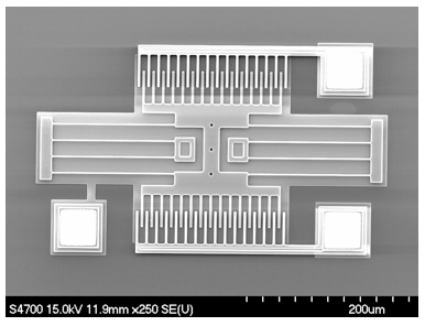
A surface micromachined resonator fabricated by the MNX. This device can be
used as both a microsensor as well as a microactuator.
This vision of MEMS whereby microsensors, microactuators and microelectronics and other technologies, can be integrated onto a single microchip is expected to be one of the most important technological breakthroughs of the future. This will enable the development of smart products by augmenting the computational ability of microelectronics with the perception and control capabilities of microsensors and microactuators. Microelectronic integrated circuits can be thought of as the "brains" of a system and MEMS augments this decision-making capability with "eyes" and "arms", to allow microsystems to sense and control the environment. Sensors gather information from the environment through measuring mechanical, thermal, biological, chemical, optical, and magnetic phenomena. The electronics then process the information derived from the sensors and through some decision making capability direct the actuators to respond by moving, positioning, regulating, pumping, and filtering, thereby controlling the environment for some desired outcome or purpose. Furthermore, because MEMS devices are manufactured using batch fabrication techniques, similar to ICs, unprecedented levels of functionality, reliability, and sophistication can be placed on a small silicon chip at a relatively low cost. MEMS technology is extremely diverse and fertile, both in its expected application areas, as well as in how the devices are designed and manufactured. Already, MEMS is revolutionizing many product categories by enabling complete systems-on-a-chip to be realized.
Nanotechnology is the ability to manipulate matter at the atomic or molecular level to make something useful at the nano-dimensional scale. Basically, there are two approaches in implementation: the top-down and the bottom-up. In the top-down approach, devices and structures are made using many of the same techniques as used in MEMS except they are made smaller in size, usually by employing more advanced photolithography and etching methods. The bottom-up approach typically involves deposition, growing, or self-assembly technologies. The advantages of nano-dimensional devices over MEMS involve benefits mostly derived from the scaling laws, which can also present some challenges as well.
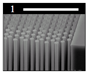
An array of sub-micron posts made using top-down nanotechnology fabrication
methods.
Some experts believe that nanotechnology promises to: a). allow us to put essentially every atom or molecule in the place and position desired – that is, exact positional control for assembly, b). allow us to make almost any structure or material consistent with the laws of physics that can be specified at the atomic or molecular level; and c). allow us to have manufacturing costs not greatly exceeding the cost of the required raw materials and energy used in fabrication (i.e., massive parallelism).
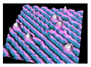
A colorized image of a scanning-tunneling microscope image of a surface,
which is a common imaging technique used in nanotechnology.
Although MEMS and Nanotechnology are sometimes cited as separate and distinct technologies, in reality the distinction between the two is not so clear-cut. In fact, these two technologies are highly dependent on one another. The well-known scanning tunneling-tip microscope (STM) which is used to detect individual atoms and molecules on the nanometer scale is a MEMS device. Similarly the atomic force microscope (AFM) which is used to manipulate the placement and position of individual atoms and molecules on the surface of a substrate is a MEMS device as well. In fact, a variety of MEMS technologies are required in order to interface with the nano-scale domain.
Likewise, many MEMS technologies are becoming dependent on nanotechnologies for successful new products. For example, the crash airbag accelerometers that are manufactured using MEMS technology can have their long-term reliability degraded due to dynamic in-use stiction effects between the proof mass and the substrate. A nanotechnology called Self-Assembled Monolayers (SAM) coatings are now routinely used to treat the surfaces of the moving MEMS elements so as to prevent stiction effects from occurring over the product’s life.
Many experts have concluded that MEMS and nanotechnology are two different labels for what is essentially a technology encompassing highly miniaturized things that cannot be seen with the human eye. Note that a similar broad definition exists in the integrated circuits domain which is frequently referred to as microelectronics technology even though state-of-the-art IC technologies typically have devices with dimensions of tens of nanometers. Whether or not MEMS and nanotechnology are one in the same, it is unquestioned that there are overwhelming mutual dependencies between these two technologies that will only increase in time. Perhaps what is most important are the common benefits afforded by these technologies, including: increased information capabilities; miniaturization of systems; new materials resulting from new science at miniature dimensional scales; and increased functionality and autonomy for systems.
Whether you are interested in developing MEMS or nano-devices, the MNX is the world’s leading fabricator for these technologies and can help you with your development or research project. Please contact us at engineering@mems-exchange.org or 703-262-5368 for more information.