Fabricating MEMS and Nanotechnology
MEMS fabrication is an extremely exciting endeavor due to the customized nature of process technologies and the diversity of processing capabilities. MEMS fabrication uses many of the same techniques that are used in the integrated circuit domain such as oxidation, diffusion, ion implantation, LPCVD, sputtering, etc., and combines these capabilities with highly specialized micromachining processes. Some of the most widely used micromachining processes are discussed below.
Note: the MNX has more expertise and knowledge in MEMS and Nanotechnology fabrication than anyone in the world. We can help you save time, money and frustration. If you have specific questions about fabrication, contact us at engineering@mems-exchange.org or at 703-262-5368.
Bulk Micromachining
The oldest micromachining technology is bulk micromachining. This technique involves the selective removal of the substrate material in order to realize miniaturized mechanical components. Bulk micromachining can be accomplished using chemical or physical means, with chemical means being far more widely used in the MEMS industry.
A widely used bulk micromachining technique is chemical wet etching, which involves the immersion of a substrate into a solution of reactive chemical that will etch exposed regions of the substrate at measurable rates. Chemical wet etching is popular in MEMS because it can provide a very high etch rate and selectivity. Furthermore, the etch rates and selectivity can be modified by: altering the chemical composition of the etch solution; adjusting the etch solution temperature; modifying the dopant concentration of the substrate; and modifying which crystallographic planes of the substrate are exposed to the etchant solution.
There are two general types of chemical wet etching in bulk micromachining: isotropic wet etching and anisotropic wet etching. In isotropic wet etching, the etch rate is not dependent on the crystallographic orientation of the substrate and the etching proceeds in all directions at equal rates. In theory, lateral etching under the masking layer etches at the same rate as the etch rate in normal direction. However, in practice lateral etching is usually much slower without stirring, and consequently isotropic wet etching is almost always performed with vigorous stirring of the etchant solution. Figure 1 illustrates the profile of the etch using an isotopic wet etchant with and without stirring of the etchant solution.
Any etching process requires a masking material to be used, with preferably a high selectivity relative to the substrate material. Common masking materials for isotropic wet silicon etching include silicon dioxide and silicon nitride. Silicon nitride has a much lower etch rate compared to silicon dioxide and therefore is more frequently used.
The etch rate of some isotropic wet etchant solution mixtures are dependent on the dopant concentration of the substrate material. For example: the commonly used mixture of HC2H3O2:HNO3:HF in the ratio of 8:3:1 will etch highly doped silicon (> 5 x 10¹⁸ atoms/cm3) at a rate of 50 to 200 microns/hour, but will etch lightly doped silicon material at a rate 150 times less. Nevertheless, the etch rate selectivity with respect to dopant concentration is highly dependent on solution mixture.
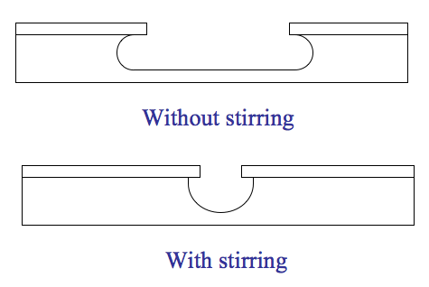
Figure 1: Illustration of the etch profile, with and without stirring,
using an isotropic wet chemical etchant.
The much more widely used wet etchants for silicon micromachining are anisotropic wet etchants. Anisotropic wet etching involves the immersion of the substrate into a chemical solution wherein the etch rate is dependent on crystallographic orientation of the substrate. The mechanism by which the etching varies according to silicon crystal planes is attributed to the different bond configurations and atomic density that the different planes exposed to the etchant solution. Wet anisotropic chemical etching is typically described in terms of etch rates according to the different normal crystallographic places, usually <100>, <110>, and <111>. In general, silicon anisotropic etching etches more slowly along the <111> planes than all the other planes in the lattice and the difference in etch rate between the different lattice directions can be as high as 1000 to 1. It is thought that the reason for the slower etch rate of the <111> planes is that these planes have the highest density of exposed silicon atoms in the etchant solution, as well as 3 silicon bonds below the plane, thereby leading to some amount of chemical shielding of the surface.
The ability to delineate the different crystal planes of the silicon lattice in anisotropic wet chemical etching provides a high-resolution etch capability with reasonably tight dimensional control. It also provides the ability for two-sided processing to embody self-isolated structures wherein only one side is exposed to the environment. This assists in packaging of the device and is very useful for MEMS devices exposed to harsh environments, such as pressure sensors. Anisotropic etching techniques have been around for over 25 years and are commonly used in the manufacturing of silicon pressure sensors as well as bulk micromachined accelerometers.
Figure 2 below is an illustration of some of the shapes that are possible using anisotropic wet etching of <100> oriented silicon substrates including an inverted pyramidal and a flat bottomed trapezoidal etch pit. Note that the shape of the etch pattern is primarily determined by the slower etching <111> planes. Figures 3a and 3b are SEM photographs of a silicon substrate after an anisotropic wet etching. Figure 3a shows a trapezoidal etch pit that has been subsequently diced across the etch pit and Figure 3b shows the backside of a thin membrane that could be used to make a pressure sensor. It is important to note that the etch profiles shown in the Figures are only for a <100> oriented silicon wafer; substrates with other crystallographic orientations will exhibit different shapes. Occasionally, substrates with other orientations are used in MEMS fabrication, but given the cost, lead times and availability, the vast majority of substrates used in bulk micromachining have <100> orientation.
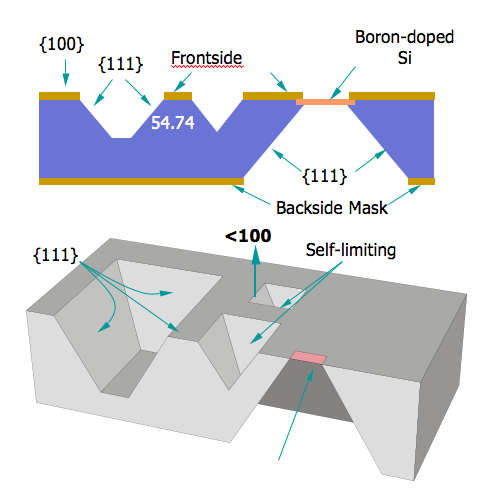
Figure 2: Illustration of shape of the etch profiles of a <100> oriented
silicon substrate after immersion in an anisotropic wet etchant solution.
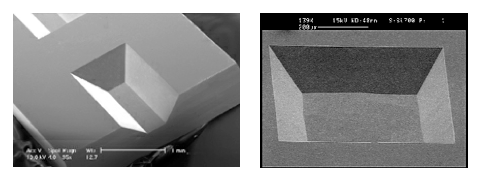
3a3b
Figures 3a and 3b: SEMS of a <100> oriented silicon substrate after
immersion in an anisotropic wet etchant.
Useful anisotropic wet etching requires the ability to successfully mask certain areas of the substrate and consequently an important criterion for selecting an etchant is the availability of good masking materials. Silicon nitride is a commonly used masking material for anisotropic wet etchants since it has a very low etch rate in most etchant solutions. Some care must be exercised in the type of silicon nitride used, since any pin hole defects will result in the attack of the underlying silicon. Also, some low-stress silicon-rich nitrides can etch at much higher rates compared to stoichiometric silicon nitride formulations. Thermally grown SiO2 is frequently used as a masking material, but some care must be exercised to ensure a sufficiently thick masking layer when using KOH etchants, since the etch rates of oxide can be high. Photoresists are unusable in any anisotropic etchant. Many metals including Ta, Au, Cr, Ag, and Cu hold up well in EDP and Al holds up in TMAH under certain conditions.
In general, the etch rate, etch rate ratios (100)/(111), and etch selectivities of anisotropic etchants are strongly dependent on chemical composition and temperature of the etchant solution.
Frequently, when using bulk micromachining it is desirable to make thin membranes of silicon or control the etch depths very precisely. As with any chemical process, the uniformity of the etching can vary across the substrate, making this difficult. Timed etches whereby the etch depth is determined by multiplying the etch rate by the etch time are difficult to control and etch depth is very dependent on sample thickness uniformity, etchant species diffusion effects, loading effects, etchant aging, surface preparation, etc. To allow a higher level of precision in anisotropic etching the MEMS field has developed solutions to this problem, namely etch stops. Etch stops are very useful to control the etching process and provide uniform etch depths across the wafer, from wafer to wafer, and from wafer lot to wafer lot. There are two basic types of etch stop methods that are used in micromachining: dopant etch stops and electrochemical etch stops.
Surface Micromachining
Surface micromachining is another very popular technology used for the fabrication of MEMS devices. There are a very large number of variations of how surface micromachining is performed, depending on the materials and etchant combinations that are used. However, the common theme involves a sequence of steps starting with the deposition of some thin-film material to act as a temporary mechanical layer onto which the actual device layers are built; followed by the deposition and patterning of the thin-film device layer of material which is referred to as the structural layer; then followed by the removal of the temporary layer to release the mechanical structure layer from the constraint of the underlying layer, thereby allowing the structural layer to move. An illustration of a surface micromachining process is shown in Figure 4, wherein an oxide layer is deposited and patterned. This oxide layer is temporary and is commonly referred to as the sacrificial layer. Subsequently, a thin film layer of polysilicon is deposited and patterned and this layer is the structural mechanical layer. Lastly, the temporary sacrificial layer is removed and the polysilicon layer is now free to move as a cantilever.
Some of the reasons surface micromachining is so popular is that it provides for precise dimensional control in the vertical direction. This is due to the fact that the structural and sacrificial layer thicknesses are defined by deposited film thicknesses which can be accurately controlled. Also, surface micromachining provides for precise dimensional control in the horizontal direction, since the structural layer tolerance is defined by the fidelity of the photolithography and etch processes used. Other benefits of surface micromachining are that a large variety of structure, sacrificial and etchant combinations can be used; some are compatible with microelectronics devices to enable integrated MEMS devices. Surface micromachining frequently exploits the deposition characteristics of thin-films such as conformal coverage using LPCVD. Lastly, surface micromachining uses single-sided wafer processing and is relatively simple. This allows higher integration density and lower resultant per die cost compared to bulk micromachining.
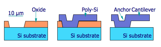
Figure 4: Illustration of a surface micromachining process.
One of the disadvantages of surface micromachining is that the mechanical properties of most deposited thin-films are usually unknown and must be measured. Also it is common for these types of films to have a high state of residual stress, frequently necessitating a high temperature anneal to reduce residual stress in the structural layer. Also, the reproducibility of the mechanical properties in these films can be difficult to achieve. Additionally, the release of the structural layer can be difficult due to a stiction effect whereby the structural layer is pulled down and stuck to the underlying substrate due to capillary forces during release. Stiction can also occur in use and an anti-stiction coating material may be needed.
The most commonly used surface micromachining process and material combination is a PSG sacrificial layer, a doped polysilicon structural layer, and the use of Hydrofluoric acid as the etchant to remove the PSG sacrificial layer and release the device. This type of surface micromachining process is used to fabricate the Analog Devices integrated MEMS accelerometer device used for crash airbag deployment. Figure 5 and Figure 6 are SEMs of two surface micromachined polysilicon MEMS devices.
Another variation of the surface micromachining process is to use a metal structural layer, a polymer layer as the sacrificial layer, and an O2 plasma as the etchant. The advantage of this process is that the temperature of the sacrificial and structural layer depositions are sufficiently low so as not to degrade any microelectronics in the underlying silicon substrate, thereby integrating MEMS with electronics. Also, since the sacrificial layer is removed without immersion in a liquid, problems associated with stiction during release are avoided. A process similar to this is used to produce the Texas Instruments Digital Light Processor (DLP) device used in projection systems.
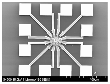
Figure 5: Polysilicon micromotor fabricated using a surface micromachining
process.
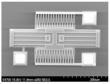
Figure 6: Polysilicon resonator structure fabricated using a surface
micromachining process.
Wafer Bonding
Wafer bonding is a micromachining method that is analogous to welding in the macroscale world and involves the joining of two (or more) wafers together to create a multi-wafer stack. There are three basic types of wafer bonding including: direct or fusion bonding; field-assisted or anodic bonding; and bonding using an intermediate layer. In general, all bonding methods require substrates that are very flat, smooth, and clean, in order for the wafer bonding to be successful and free of voids.
Direct or fusion bonding is typically used to mate two silicon wafers together or alternatively to mate one silicon wafer to another silicon wafer that has been oxidized. Direct wafer bonding can be performed on other combinations, such as bare silicon to a silicon wafer with a thin-film of silicon nitride on the surface as well.
As mentioned, wafer bonding is analogous to welding in the macroscale world. Wafer bonding is used to attach a thick layer of single crystal silicon onto another wafer. This can be extremely useful when it is desired to have a thick layer of material for applications requiring appreciable mass or in applications where the material properties of single crystal silicon are advantageous over those of thin-film LPCVD materials. Direct wafer bonding is also used to fabricate Silicon-On-Insulator (SOI) wafers having device layers several microns or more in thickness.
Another popular wafer bonding technique is anodic bonding. In anodic bonding a silicon wafer is bonded to a Pyrex 7740 wafer using an electric field and elevated temperature. The two wafers can be pre-processed prior to bonding and can be aligned during the bonding procedure. The mechanism by which anodic bonding works is based on the fact that Pyrex 7740 has a high concentration of Na+ ions; a positive voltage applied to the silicon wafer drives the Na+ ions from the Pyrex glass surface, thereby creating a negative charge at glass surface. The elevated temperature during the bonding process allows the Na+ ions to migrate in the glass with relative ease. When the Na+ ions reach the interface, a high field results between silicon and glass, and this combined with the elevated temperatures fuses the two wafers together. As with direct wafer bonding, it is imperative that the wafers are flat, smooth, and clean and that the anodic bonding process is performed in a very clean environment. An advantage of this process is that Pyrex 7740 has a thermal expansion coefficient nearly equal to silicon and therefore there is a low value of residual stress in the layers. Anodic bonding is a widely used technique for MEMS packaging.
In addition to direct and anodic bonding there are other wafer bonding techniques that are used in MEMS fabrication. One method is eutectic bonding and involves the bonding of a silicon substrate to another silicon substrate at an elevated temperature using an intermediate layer of gold on the surface of one of the wafers. Eutectic bonding works because the diffusion of gold into silicon is extremely rapid at elevated temperatures. In fact this is a preferred method of wafer bonding at relatively low temperatures.
Another wafer bonding technique used in MEMS is glass frit bonding. In this process a glass is spun or screen-printed onto a substrate surface. Subsequently this wafer is physically contacted to another wafer and the composite is annealed to flow the glass intermediate layer and bond the two wafers.
Lastly, various polymers can be used as intermediate layers to bond wafers including epoxy resins, photoresists, polyimides, silicones, etc. This technique is commonly used during various fabrication steps in MEMS such as when the device wafer becomes too fragile to handle without mechanical support.
High-Aspect Ratio MEMS Fabrication Technologies
Deep Reactive Ion Etching of Silicon
Deep reactive ion etching or DRIE is a relatively new fabrication technology that has been widely adopted by the MEMS community. This technology enables very high aspect ratio etches to be performed into silicon substrates. The sidewalls of the etched holes are nearly vertical and the depth of the etch can be hundreds or even thousands of microns into the silicon substrate.
Figure 7 illustrates how deep reactive ion etching is accomplished. The etch is a dry plasma etch and uses a high density plasma to alternately etch the silicon and deposit an etch resistant polymer layer on the sidewalls. The etching of the silicon is performed using a SF6 chemistry whereas the deposition of the etch resistant polymer layer on the sidewalls uses a C4F8 chemistry. Mass flow controllers alternate back and forth between these two chemistries during the etch. The protective polymer layer is deposited on the sidewalls as well as on the bottom of the etch pit, but the anisotropy of the etch removes the polymer at the bottom of the etch pit faster than the polymer is removed from the sidewalls. The sidewalls are not perfected or optically smooth and if the sidewall is magnified under SEM inspection, a characteristic washboard or scalloping pattern is seen in the sidewalls. The etch rates on most commercial DRIE systems varies from 1 to 4 microns per minute. DRIE systems are single wafer tools. Photoresist can be used as a masking layer for DRIE etching. The selectivity with photoresist and oxide is about 75 to 1 and 150 to 1, respectively. For a through wafer etch a relatively thick photoresist masking layer will be required. The aspect ratio of the etch can be as high as 30 to 1, but in practice tends to be 15 to 1. The process recipe depends on the amount of exposed silicon due to loading effects in the system, with larger exposed areas etching at a much faster rate compared to smaller exposed areas. Consequently, the etch must frequently be characterized for the exact mask feature and depth to obtain desirable results.
Figure 8 is a SEM of a MEMS component fabricated using DRIE and wafer bonding. This device was made using an SOI wafer wherein a backside etch was performed through the handle wafer, stopping on the buried oxide layer, and a frontside DRIE was performed on the SOI device layer. Then the buried oxide was removed to release the microstructure, allowing it to freely move.
Figure 9 is a cross section SEM of a silicon microstructure fabricated using DRIE technology. As can be seen, the etch is very deep into the silicon substrate and the sidewalls are nearly vertical.
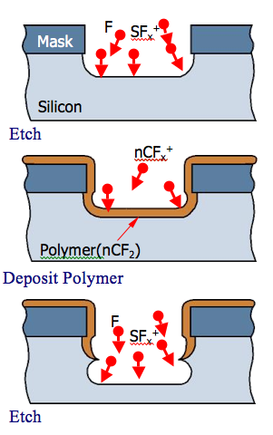
Figure 7: Illustration of how deep reactive ion etching works.
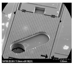
Figure 8: SEM of a MEMS device fabricated using two sided DRIE etching
technology on an SOI wafer.
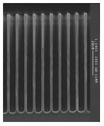
Figure 9: SEM of the cross section of a silicon wafer demonstrating
high-aspect ratio and deep trenches that can be fabricated using DRIE
technology.
Deep Reactive Ion Etching of Glass
Glass substrates can also be etched deep into the material with high aspect ratios and this technology has been gaining in popularity in MEMS fabrication. Figure 10 shows a structure fabricated into glass using this technology. The typical etch rates for high aspect ratio glass etching range between 250 and 500 nm per minute. Depending on the depth of the photoresist, metal or a polysilicon can be used as a mask.
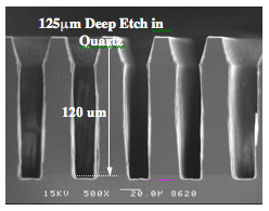
Figure 10: SEM of high aspect ratio structures etched into a glass
substrate fabricated by MNX.
LIGA
Another popular high aspect ratio micromachining technology is called LIGA, which is a German acronym for “LIthographie Galvanoformung Adformung.” This is primarily a non-silicon based technology and requires the use of synchrotron generated x-ray radiation. The basic process is outlined in Figure 11 and starts with the cast of an x-ray radiation sensitive PMMA onto a suitable substrate. A special x-ray mask is used for the selective exposure of the PMMA layer using x-rays. The PMMA is then developed and will be defined with extremely smooth and nearly perfectly vertical sidewalls. Also, the penetration depth of the x-ray radiation into the PMMA layer is quite deep and allows exposure through very thick PMMA layers, up to and exceeding 1 mm. After the development, the patterned PMMA acts as a polymer mold and is placed into an electroplating bath and Nickel is plated into the open areas of the PMMA. The PMMA is then removed, thereby leaving the metallic microstructure (Figure 12).
Because LIGA requires a special mask and a synchrotron (X-ray) radiation source for the exposure, the cost of this process is relatively expensive. A variation of the process which reduces the cost of the micromachined parts made with this process is to reuse the fabricated metal part (step 5) as a tool insert to imprint the shape of the tool into a polymer layer (step 3), followed by electroplating of metal into the polymer mold (step 4) and removal of the polymer mold (step 5). Obviously this sequence of steps eliminates the need for a synchrotron radiation source each time a part is made and thereby significantly lowers the cost of the process. The dimensional control of this process is quite good and the tool insert can be used many times before it is worn out.
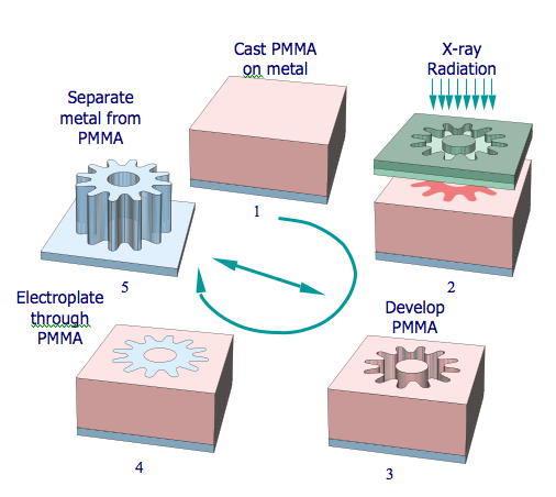
Figure 11: An illustration of the steps involved in the LIGA process to
fabricate high aspect ratio MEMS devices.
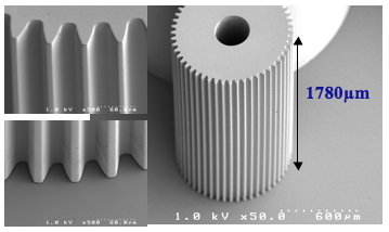
Figure 12: A tall, high aspect ratio gear made using LIGA technology.
Hot Embossing
A process to replicate deep high-aspect ratio structures in polymer materials is to fabricate the metal tool insert using LIGA or a comparable technology and then to emboss the tool insert pattern into a polymer substrate, which is then used as the part. Figure 13 is a diagram illustrating the hot embossing process. A mold insert is made using an appropriate fabrication method (shown in black cross-hatched pattern) having the inverse pattern made into it. The mold insert is placed into a hot embossing system (see Figure 14 for a photo of a hot embosser) that includes a chamber in which a vacuum can be drawn. The substrate and polymer are heated to above the glass transition temperature, Tg, of the polymer material and the mold insert is pressed into the polymer substrate. The vacuum is critical for the polymer to faithfully replicate the features in the mold insert since otherwise air would be trapped between the two surfaces resulting in distorted features. Subsequently, the substrates are cooled to below the glass transition temperature of the polymer material and force is applied to de-emboss the substrates. As shown in Figure 15, hot embossing can successfully replicate complicated, deep and high-aspect ratio features. This process can make imprints into a polymer hundreds of microns deep with very good dimensional control. The advantage of this process is that the cost of the individual polymer parts can be very low compared to the same structures made using other technologies. Because of the overwhelming cost advantages combined with very good performance, this polymer molding process is very popular for producing microfluidic components for medical applications.
Heat plastic substrate and mold insert to above plastic Tg, pull vacuum on chamber. Apply forces to emboss plastic substrate. Cool plastic substrate and mold insert to de-molding temperature and apply force to de-emboss.
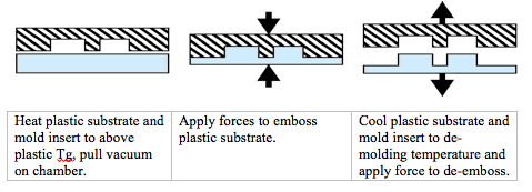
Figure 13: Illustration of the hot embossing process to create
microdevices. (Courtesy of the MNX at CNRI).
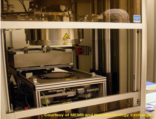
Figure 14: Photograph of a hot embossing platform during use.
(Courtesy of
the MNX at CNRI).
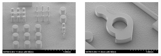
Figure 15: SEM of a variety of small test structures made in a plastic
substrate using hot embossing technology at the MNX.
The height of the plastic microstructures is nearly 300 um and the
smallest features have a diameter of about 25 um. (Courtesy of the MNX at CNRI).
Other Micromachining Technologies
In addition to bulk micromachining, surface micromachining, wafer bonding, and high aspect ratio micromachining technologies, there are a number of other techniques used to fabricate MEMS devices.
XeF2 Dry Phase Etching
Xenon Difluoride (XeF2) in a vapor state is an isotropic etchant for silicon. This etchant is highly selective with respect to other materials commonly used in microelectronics fabrication including: LPCVD silicon nitride, thermal SiO2, aluminum, titanium and others. Since this etchant is a completely dry release process, it does not suffer from the stiction problems of wet release processes. This etchant is popular with micromachining of microstructures in pre-processed CMOS wafers where openings in the passivation layers on the surface of the substrate are made to expose the silicon for etching.
Electro-Discharge Micromachining
Electro-discharge micromachining or micro-EDM is a process used to machine a conductive material using electrical breakdown discharges to remove material. A working electrode is made from a metal material onto which high voltage pulses are applied. The working electrode is brought into close proximity to the material to be machined, which is immersed in a dielectric fluid. The minimum sized features that can be made with micro-EDM are dependent on the size of the working electrode and how it is fixtured, but holes as small as tens of microns have been made using this method. One issue with micro-EDM is that it is a slow serial process.
Laser Micromachining
Lasers can generate an intense amount of energy in very short pulses of light and direct that energy onto a selected region of material for micromachining. Among the many types of lasers now in use for micromachining include: CO2, YAG, excimer, etc. Each has its own unique properties and capabilities suited to particular applications. Factors that determine the type of laser to use for a particular application include laser wavelength, energy, power, and temporal and spatial modes; material type; feature sizes and tolerances; processing speed; and cost. The action of CO2 and Nd:YAG lasers is essentially a thermal process, whereby focusing optics are used to direct a predetermined energy/power density to a well-defined location on the work piece to melt or vaporize the material. Another mechanism, which is nonthermal and referred to as photoablation, occurs when organic materials are exposed to ultraviolet radiation generated from excimer, harmonic YAG, or other UV source. Similar to microEDM, laser micromachining can produce features on the order of tens of microns, but it is a serial process and therefore slower.
Focused Ion Beam Micromachining
Another versatile tool for performing micromachining is the focused ion beam (FIB). The accelerating voltages are adjustable from a few keV to several hundred keV. The spot sizes can be focused down to below 25 nm, making it capable of producing extremely small structures. The user can input a 3-D CAD solid model of desired etching topology; the computer-controlled stage with sub-micron positional accuracy allows very precise registration of sample. In addition to material removal, the FIB can also be used to perform ion induced deposition, lithography, implantation doping, mask repair, device repair, and device diagnostics. Many of these tools can also be outfitted with a secondary column for mass analysis of particles removed from the substrate using uSIMS.
MEMS Process Integration
Process integration for our purposes is defined as understanding, characterizing and optimizing to the extent possible, the interrelationship of the individual processing steps in a process sequence. Given the customization of MEMS process sequences, it should not be surprising that process integration is of critical importance. Also, MEMS developers must have good data on the electrical materials properties as well as data on the mechanical material properties. Coupled with the enormous diversity of materials and processing techniques used in MEMS fabrication, means that process integration can be a major part of a product development effort. Fortunately, the MNX has been working on this problem and has developed project-tested solutions so as to simultaneously provide the flexibility in the process sequence that is needed in MEMS while also affording a good level of reproducibility.
Advantages of MEMS and Nano Manufacturing There are many beneficial attributes of MEMS and Nanotechnology. Firstly, these devices are made using integrated circuit-like processes, which enables the ability to integrate multiple functionalities onto a single microchip. The ability to integrate miniaturized sensors, miniaturized actuators and miniaturized structures along with microelectronics has far-reaching implications in countless products and applications.
Secondly, MEMS and Nanotechnology borrow many of the production techniques of batch fabrication from the integrated circuit industry and therefore, the per-unit device or microchip cost of complex miniaturized electromechanical systems can be radically reduced - similar to the per die cost reductions we have experienced in the IC industry. Although the cost of the production equipment and each wafer can be relatively high, the fact that this cost can be spread over many die in batch fabrication production can drastically lower the per part cost.
Thirdly, integrated circuit fabrication techniques coupled with the tremendous advantages of silicon and many other thin-film materials in mechanical applications allows the reliability of miniaturized electromechanical systems to be radically improved. It is well known that the most expensive and most unreliable components of a conventional macroscale control system are the sensors and actuators. It is expected that as these miniaturized sensors and actuators are integrated onto a single microchip with electronics, we will see similar improvements in system reliability such as we have experienced in the transition from discrete electronics on a printed circuit board to integrated circuits. The lower cost of these miniaturized electromechanical systems also allows them to be easily and massively deployed and more easily maintained and replaced as needed.
Fourthly, miniaturization of micro- and nanosystems enables many benefits including: increased portability, lower power consumption, and the ability to place radically more functionality in a smaller amount of space and without any increase in weight.
Fifthly, the ability to make the signal paths smaller and place radically more functionality in a small amount of space allows the overall performance of electromechanical systems to be enormously improved.
In short, MEMS and Nanotechnology translates into products that have lower cost, higher functionality, improved reliability and increased performance.
If you have questions about the advantages offered by MEMS or Nanotechnology, contact us at engineering@mems-exchange.org or at 703-262-5368.