SEM06.jpgMEMS Exchange Handout.jpg- A MEMS Exchange Information Image
MEMS LIGA.jpg- LIGA stands for X-ray LIthography, Electroforming (German: Galvanoformung), and molding (German: Abformung). This technology allows us to define high aspect ratio structures in nickel. The process consists of exposing a sheet of PMMA bonded to a wafer using X-ray lithography. The PMMA is then developed and the exposed material is removed. Nickel is then electroplated up in the open areas of the PMMA. The nickel over-plate is removed by polishing, leaving high aspect ratio nickel parts. The PMMA is removed, and the nickel parts may remain anchored to the substrate or be released.
MEMS Silicon DRIE.jpg- Deep reactive ion etching is a process used to etch substrates to form deep cavities with relatively high aspect ratio (10-20). Most Deep RIE systems use the so-called "Bosch process" in which a fluor polymer is used to passivate the etching of the sidewalls.
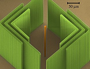
MEMS SU8 High Aspect Ratio.jpg- The image is a colorized Scanning Electron Micrograph (SEM) of microstructure made using extremely short wavelength exposure techniques of a thick radiation sensitive polymer layer which was spun onto the substrate and developed after exposure to reveal an extraordinarily high aspect ratio microstructure. The central post (shown in orange) is hundreds of microns tall and only a few microns in diameter. The surrounding angular shaped structures are also a few microns wide, separated from one another by a few microns, and are also hundreds of microns tall. This structure was made through the MEMS and Nanotechnology Exchange fabrication network.
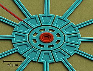
MEMS Motor SEM.jpg- The image is a colorized Scanning Electron Micrograph (SEM) of a salient-pole electrostatically actuated micromotor made from polycrystalline silicon using surface micromachining techniques. The central rotating element of the motor (e.g., the rotor) is the circular structure in the middle (shown in blue) held to the substrate by the central bearing (which is shown in red). Properly phased voltage potentials are placed on the motor stators (typically 120 degrees advanced in phase sequentially around the stators), which are equally spaced around the perimeter of the rotor (also shown in blue) and these applied voltages on the stators cause the central rotor to turn around the bearing at extremely high angular velocities. This device was made through the MEMS and Nanotechnology Exchange fabrication network.
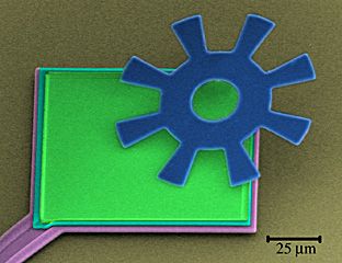
MEMS Gear SEM.jpg- This whimsical image is a colorized Scanning Electron Micrograph (SEM) of mechanical gear which is smaller than a human hair. The gear was made polycrystalline silicon using surface micromachining techniques and is no longer attached to the substrate. However, the gear did eventually lodge onto an electrical bond pad (shown in green) due to surface forces. This image illustrates the extraordinary capability of MEMS technology to enable the realization of extremely small mechanical elements. This device was made through the MEMS and Nanotechnology Exchange fabrication network.
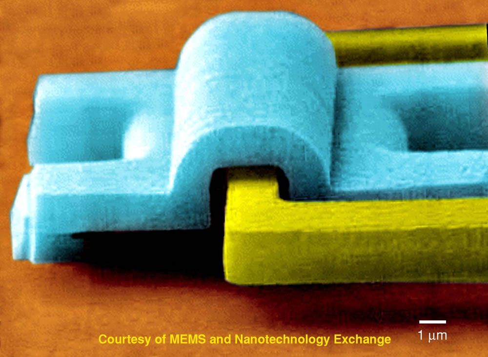
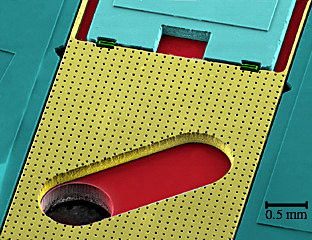
MEMS SOI SEM.jpg- The image is a colorized Scanning Electron Micrograph (SEM) of a high-aspect ratio MEMS device fabricated out of single-crystal silicon by the MEMS and Nanotechnology Exchange fabrication network. The device itself is made from a Silicon-On-Insulator (SOI) wafer where a relatively thick single-crystal silicon device layer (shown in yellow and blue in the image) has been etched into a complex micromechanical element that can move under force. The underlying area, shown in red in the image, is the SOI handle wafer which also has been etched to form a circular hole completely through the substrate. This image demonstrates the complexity of micromechanical devices that can be realized using the MEMS and Nanotechnology Exchange.
more