3. Introduction to Lithographic Equipment
3.1. The Contact Aligner (Front, back-IR and back-Optical)
The contact aligner is a tool that performs alignment and exposure of wafers. The features on the contact aligner mask are the same size as they should be on the wafer (i.e. 1x magnification). Pattern transfer takes place by printing, i.e. by placing the mask in direct contact with the surface of the wafer, and then exposing (as shown in figure 11).
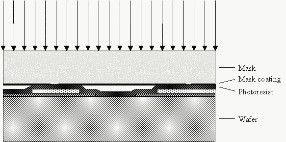
Fig. 11. Contact aligner lithography
There are two contact modes for the mask and wafer, hard and soft contact. Hard contact mode is exactly that, force is applied to push the wafer and mask together to achieve a good physical connection. The force insures that the pattern on the mask is as close as possible to the resist to be exposed, and therefore achieves good pattern transfer. The physical nature of the hard contact mode results in masks becoming dirty and degrading. Soft contact mode also results in the mask and wafer being in direct contact, but without as much force. The reduced force means that in some regions the wafer and mask may not be in direct contact, and it is possible to experience pattern transfer degradation (as diffraction effects may occur at the edges). Mask lifetimes are longer when soft contact is used. The depth of focus of the contact aligner is limited, and only the topmost layer on a wafer may be "focused "on. This means that high aspect ratio features may experience good pattern transfer at the top of the features, but this will degrade for features on lower levels.
Contact aligners often support both 'front to front' and 'front to back' alignment. This means that a mask applied to the front of the wafer may be aligned to features either on the front or back of the wafer respectively. The features used for aligning the wafer and mask are viewed through optics or a video system. The mask and wafer are aligned by bringing them close to one another (but not into contact), and then moving the wafer relative to the mask until aligned. As there are no optics between the mask and wafer, the mask must contain an alignment feature that can be aligned to the alignment mark on the wafer. This feature will then be printed onto the wafer.
When designing alignment marks it is important to consider the field of view of the alignment system to ensure that all the elements to be used in concert are visible at once (as shown in figure 7). Note that the alignment systems typically have two sets of optics to view two sets of alignment marks at once (one on the left hand side of the wafer and one on the right). Typically one set of alignment marks is used to correct for x and y translations, and then both sets are considered to remove the rotational translation (theta, as shown in figure 4).
For 'front to front' alignment (i.e. side exposed is the side mask is aligned to), the mask and wafer are both viewed through the same set of optics. The mask and wafer are moved relative to one another until they are aligned. Because a single set of optics is used, it is important that there are large open windows in the alignment mark, so that the features on the wafer can be viewed through it (as shown in figure 12). If the mask doesn't contain these open regions, it can be incredibly difficult to find the alignment mark on the wafer, making the process error prone. In some cases it is wise to include pointers on the wafer to direct the person aligning the wafer and mask to the alignment mark on the wafer. During layout, it is necessary to consider whether the mask will be clearfield or darkfield before creating the windows through which the wafer may be viewed, to ensure that they are transparent on the mask.
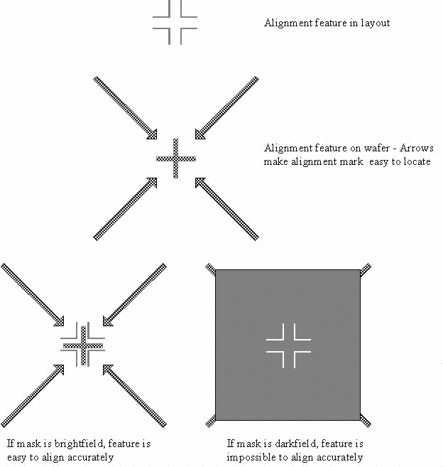
Fig. 12. Designing alignment marks so that they may be easily located and aligned.
There are two commonly used schemes for 'front to back' alignment. Many systems use infrared (IR) light to illuminate features on the back of the wafer so that they may be visible on the other side of the wafer (as silicon is somewhat transparent to IR). An IR video system is required to view the IR radiation, but alignment takes place in essentially the same manner as in front to front alignment, except that the features viewed are on the other side of the wafer, viewed through the wafer (as shown in figure 13). The constraints on the mask are similar to those for front to front alignment (i.e. need a window to see the alignment mark on the wafer). The alignment features on the wafer should be large and distinct, as there is some degradation of the wafer alignment feature image when looking through the wafer. It is also important that the wafer not have any IR-opaque layers (such as aluminum) on either side of the wafer in the alignment mark regions, as these will obscure the alignment marks, preventing alignment.
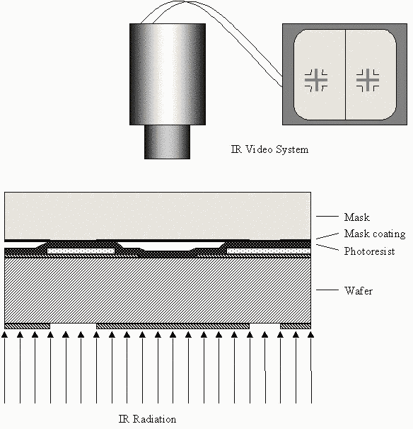
Fig. 13. IR illuminated for 'front to back' alignment
Another common scheme for performing 'front to back' alignment is to have two sets of aligned optics, one for the top and one for the bottom of the wafer. The aligned optic images are combined into a single overlay image, so that the top image may be aligned to the bottom by moving the mask and wafer relative to one another. As the images of the back surface of the wafer and the mask are acquired separately and then combined, the mask and wafer are not constrained like in other alignment modes (as don't have to be able to locate and see alignment mark through the mask and/or wafer).
When would I want to use contact lithography?
If you require the capability of aligning features on the back of the wafer with features on the front of the wafer, the contact aligner is the most straightforward choice (although Electronic Visions now makes a 1x stepper with front-back alignment capability). The contact aligner is not capable of resolving as high resolution features as other lithography techniques (at best capable of 1um features, typically 3um). It is more suitable for applications with thicker resists than steppers are, and for more extreme topographies as it has a better depth of focus. The contact aligner is a relatively low cost method of performing lithography.
The contact aligner mask uniquely addresses every location on the wafer, which allows the entire wafer to be patterned with a large single continuous feature. The wafer may also be covered with dies, each of which may be completely unique, or even have a mix of large features and dies. This makes the contact aligner uniquely flexible.
3.2. Stepper (Step and Repeat Projector)
A stepper is quite different from a contact aligner, in that a stepper uses a mask (called a reticle) to expose a single die at a time on the wafer. The dies are tiled to cover the entire surface of the wafer (as shown in figure 14). It steps from die location to die location reusing the same reticle until the entire wafer is exposed, rather than having a wafer size mask, and exposing the entire wafer at once. The reticle doesn't make contact with the wafer, but rather light is projected through the reticle and onto the wafer. The light is focused using the projection optics. A reduction stepper is a stepper where the image on the reticle is larger than the desired image on the wafer, and the image is reduced by the projection optics before it reaches the wafer. The advantage of this system is that the resolution of the lithography step is not limited by the resolution of the reticle. The most common reduction steppers are 4x, 5x and 10x reduction magnifications.
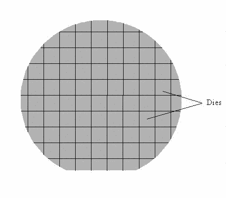
Fig. 14. Die patterns on a wafer
In the case of a 1x stepper, as the layout is the size of a die, if the die is moderately sized, it is possible in some cases to have the die layout for multiple layers on a single reticle, thus reducing the reticle cost. The area on the reticle pertaining to the current layer is then projected onto the wafer.
As a stepper pattern is stepped to multiple points on a wafer, the alignment process is a little less intuitive. Firstly, the reticle is aligned to the stepper column. In order to do this, the reticle must have a set of fiducials (alignment marks) that are compatible with the stepper to be used. (Please see the MNX template download page for fiducials for the steppers available through the MEMS and Nanotechnology Exchange.) The fiducials are located on the reticle outside of the area that is printed on the wafer, so they are not transferred to the wafer during exposure (as shown in figures 15 a and b). The reticle is now aligned to the stepper column. Next we align the column to the wafer, and hence the reticle will be aligned to the wafer.
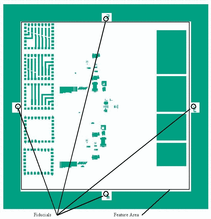
Fig. 15a. Fiducial Location and feature area
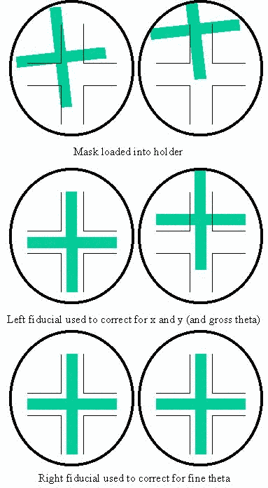
Fig. 15b. Reticle alignment to stepper column
For the first lithography on a wafer, the wafer is aligned with respect to its flat,. The exposure pattern (die pattern) is entered by the technician, and the wafer is exposed (die by die). If the pattern defined in the first exposure will be aligned to in future lithography modules, then the first layer must contain alignment marks. The alignment marks must be compatible with the stepper, as the optics for aligning the wafer are referenced to features in the stepper alignment optics. Typically two alignment marks are used (as in the contact aligner) to align the wafer, one alignment mark is used to correct for x and y translations, and both are considered to remove the rotational translation (theta). As the pattern on the wafer is repeated, the reticle only needs to contain a single alignment mark, as the alignment marks in two different dies are used to align the wafer (as shown in figure 16). As the wafer alignment optics may have limited travel, in order to ensure that the alignment marks are positioned to line up with the alignment optics, it may be necessary to either space the die appropriately, or alternatively have two alignment marks per die. It is necessary to indicate the offset of the alignment mark from the center of the reticle (i.e. offset from the center of the fiducials), as the tool references the reticle image to the wafer with respect to the center of the reticle. It is simplest if the alignment mark falls in the center of the reticle. It is assumed that the center of the fiducials is the center of the reticle. If there is a shift of the whole pattern (i.e. such that the alignment mark is at the center of the fiducials, but not at the center of the reticle), it is possible that there will not be enough travel in the mask alignment stage to allow the alignment to take place.
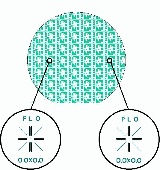
Fig. 16. Alignment of the wafer to the stepper column
If the wafer is to experience significant processing, it may be necessary to include alignment marks in other layers, in case the original set are degraded by subsequent processing. It is important to label all alignment marks with the name of the layer they appear in, and their offset from the center of the reticle (it is not recommended to place alignment marks on top of one another).
When would I want to use step and repeat lithography?
The step and repeat projector, allows a single pattern to be repeatedly printed, die by die, across a wafer. In production lithography it is very advantageous to have many identical devices on a single wafer. It is possible to switch reticles and selectively expose die, so that different patterns are used on different die; however this is complicated and error prone. This is a moderately priced lithography technique.
In the case of a 1x stepper, the resolution of the tool is comparable to a contact aligner. The disadvantage of the stepper is that the wafer may only be exposed die by die, without a gain in resolution. However, as the die usually represents a small fraction of the surface area of the reticle, in some cases multiple die patterns can be included on a single reticle, which reduces the cost for the reticle set.
Reduction steppers (commonly 4x, 5x or 10x) are capable of higher resolution than contact aligners, as the reticle image is reduced when projected on the wafer. These systems routinely produce 1um and smaller features in MEMS research facilities. In IC production facilities new well characterized tools routinely produce sub-micron features. These tools are more sensitive to depth of focus than contact aligners and as a result may produce poor results on wafers with extreme topographies.
3.3. Direct Write Systems
These are systems that don't require a mask; rather the radiation source used to expose the photoresist is scanned directly on the wafer as shown in figure 17. The layout CAD is fed directly in the direct write system, and the patterning may commence once the wafer has been registered. E-beam is the most common direct write technique.
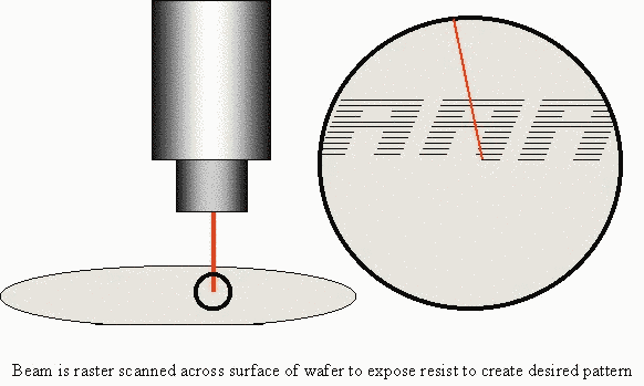
Fig. 17. Direct write patterning
When would I want to use a direct write system?
E-beam is used when very high resolution pattern definition is required. The cost of the technique scales directly with the scan time required to expose an entire wafer. The exposure time depends on the thickness of the resist layer, the amount of area to be exposed and the diameter of the beam used. Both positive and negative resists are routinely employed in order to keep the amount of surface area requiring exposure to a minimum. The minimum resist thickness suitable for the application is also used to reduce the write time. E-beam may be used for exposing thick layers with good resolution, but the cost increases dramatically with increased exposure time.
This is an expensive method of achieving pattern transfer. It also has significant limitations in that often the system may only be able to scan a small region as a contiguous unit (akin to a die). Registration of regions to one another is not as good as the feature to feature registration within a die, so stitching of fine features across region borders often can't be done seamlessly.