5. Mask Rules and Guidelines for use with the MEMS and Nanotechnology Exchange
5.1. Layout Tools
5.2. File Formats
The MNX currently has experience with CIF, GDSII, DWG and DXF layout file formats; however, we are expanding our capabilities and will try work with other formats.
5.3. Layout Layer Designations
Except in the case fixed process sequence foundry runs, users may select layer designations that suit them best. It is important however that the layer designations be communicated to the mask manufacturer, along with the information about that layer.
5.4. Design Rules
As MNX users have complete flexibility in process sequence design, design rules don't exist for almost all the process sequences available. Each base process has information about its capabilities, which should provide the user with some information as to what a process is capable of. If the user requires more detailed information than is available through the on-line database, please contact us for more information.
5.5. Conventions
5.5.1. Mask and Mask Set Names
In order to ensure that the correct mask is used for the appropriate step in a process sequence, a few basic conventions should be adhered to:
The mask name should consist of a multiple pieces of information so that it may be uniquely identified within the MNX.
The mask name should include a unique name for the mask set, such as the run number. This is necessary so the mask set can be easily distinguished from other mask sets belonging to the same user or others. The use of the run number allows the user to remain anonymous if they so desire.
The mask name should contain the name of the layer or structures which it is intended to define. If multiple masks are used to pattern a single layer, they should be discriminated with either a number designating the sequence in which they are used, or by using names unique to the function of the two masks (e.g. dimple Vs. anchor).
The mask name must be consistent with the mask name used in the runcard (obviously once the mask is made it is easier to change the runcard!).
Example mask names:
R0555 PSG0 Dimple
CNRI Device-2 Poly2-2
R0555 PPI3 Beams
5.5.2. Device Labeling
The MNX makes available a series of metrology and test equipment, either for use remotely or by an operator. In either instance it may be desirable to describe a device location to someone or something succinctly. It is therefore a good idea to include in your layout names for your devices, and the location of the device as shown in figure of 20. The center of the wafer is referenced as shown in figure 21. The center of a die is referenced to the center of the layout, as determined from the fiducials as shown in figure 22. This will allow the tracking of single devices through the entire fabrication sequence, as the associated metrology may be referenced to the performance of a specific device.
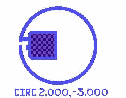
Fig. 20. Inclusion of device names and location in layout
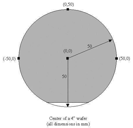
Fig. 21. Center of the wafer and coordinate system
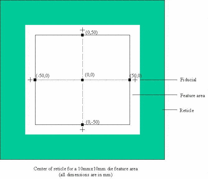
Fig. 22. Center of the reticle and die coordinate system
5.5.3. Mask Polarities and Orientation
When a mask is printed from the computer generated layout, the user typically has the option of having the features on the layout printed in lightfield or darkfield polarities as shown in figure 19. It is necessary to select the polarity to achieve the desired resist image on the wafer (depending on whether a subtractive or additive process will pattern the underlying layer, and the polarity of the resist used). This allows the user to perform the layout for either the image desired, or its negative, depending on which is easier as shown in figure 19. The convention is for desired feature polarity is positive indicates features digitized in layout will translate to the higher regions after the pattern process (as demonstrated in figure 23).
|
Desired Feature Polarity |
Resist Type |
Pattern Process |
Mask Polarity Required |
|---|---|---|---|
|
Positive |
Positive |
Subtractive (etch) |
Lightfield |
|
Positive |
Positive |
Additive (lift-off) |
Darkfield |
|
Positive |
Negative |
Subtractive (etch) |
Darkfield |
|
Positive |
Negative |
Additive (lift-off) |
Lightfield |
|
Negative |
Positive |
Subtractive (etch) |
Darkfield |
|
Negative |
Positive |
Additive (lift-off) |
Lightfield |
|
Negative |
Negative |
Subtractive (etch) |
Lightfield |
|
Negative |
Negative |
Additive (lift-off) |
Darkfield |
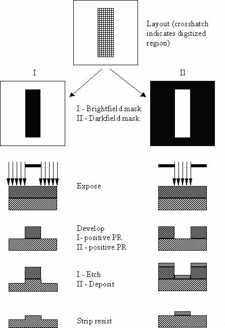
Fig. 23. Positive and negative mask polarity images
5.6. Alignment Marks for Contact Aligners
Each alignment mark should be labeled with the name of the layer in which it appears, as well as a unique identifier if multiple alignment marks appear in the same layer.
The position of the center of the alignment marks with respect to the center of the wafer (0, 0) should appear with each alignment mark so that they may be easily located (example shown in figure 21). The center of the wafer is the center of the circle circumscribed by the radius of the wafer, and therefore does not consider the effect of the flat (i.e. not the centroid of the wafer surface). If units are not specified, it will be assumed that the offset is in millimeters.
Care should be taken that subsequent processing will not completely remove an alignment mark. This may require that alignment marks in one layer be masked in other layers. Direct overlay of alignment marks on top of one another may lead to alignment mark degradation. In order to overcome this it may be necessary to have duplicate alignment marks within a layer, one for each other layer aligned to (shown in figure 24).
For wafers requiring IR front to back alignment, it is important to ensure that there are no IR-opaque layers above or below the alignment marks, to ensure they will be visible.
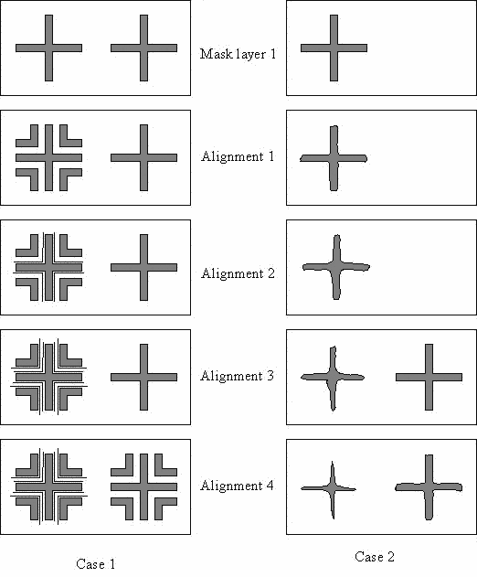
Fig. 24. Use of multiple alignment marks
Case 1 - Transfer of alignment features on mask to wafer obscures alignment structure on wafer
Case 2 - Alignment structure on wafer deteriorates with processing
5.7. Alignment Marks and Fiducials for Stepper Reticles
Each alignment mark should be labeled with the name of the layer in which it appears, as well as a unique identifier if multiple alignment marks appear in the same layer.
The position of the center of the alignment mark with respect to the center of the fiducials (0, 0) should appear with the alignment mark so that the relevant offset may be entered (as shown in figure 22). If units are not specified, it will be assumed that the offset is in millimeters.
Care should be taken that subsequent processing will not completely remove an alignment mark expected. This may require that alignment marks in one layer be masked in other layers. Direct overlay of alignment marks on top of one another may lead to alignment mark degradation. On most step and repeat tools, the wafer may be aligned and then shifted by a specified amount so that when the wafer is exposed, the pattern is not centered at the alignment mark on the wafer. This means that there is some flexibility in the location of the alignment mark.
It is important to check that your alignment mark location and die size are compatible with the die stepping distance you desire. This depends on the range of travel of the alignment optics on the stepper, so it may be necessary to include two alignment marks in each die to be able to achieve the stepping distance you require.
5.8. Recommended Test Features
A series of test structures are available from the MEMS and Nanotechnology Exchange template download page, which will aid in the optimal processing of your devices. The location of the test structures should be noted as well as the layer for which the test structure is intended (if one applies).
Alignment registration test structures - These test structures indicate how well one layer is registered to another. This structure provides invaluable information to the technician performing lithography, as if this structure indicates poor alignment, the resist will be stripped and the process repeated (before the pattern is committed to the wafer by etching or depositing).
Resolution test structures - This set of test structures gives the technician a good indication of the quality of the exposure and development steps in the lithography module. It also allows them to tweak the process to achieve the best results for the feature size you are most concerned with. These features should be placed at the same height as the features that you are most concerned with, as these features will be used to optimize focus.
Film thickness windows - It is often important to open windows in a material, so that the thickness of the underlying layer, or the thickness of the material remaining during an etch may be measured. Film thickness tools are typically capable of measuring only specific combinations of films, if capable of measuring more than one film on silicon. The window is required to accommodate the field of view of the thin film thickness measurement tool. This is often very important during etching, to check the etch rate, and to ensure that etch is done. The edges of the window may be used for step height measurements.
If there are test structures not listed here, which you find particularly useful and would like to make available to the community, please let us know.