Guide
- Deposition
- Lithography
- Etching
Lithography in the MEMS context is typically the transfer of a pattern to a photosensitive material by selective exposure to a radiation source such as light. A photosensitive material is a material that experiences a change in its physical properties when exposed to a radiation source. If we selectively expose a photosensitive material to radiation (e.g. by masking some of the radiation) the pattern of the radiation on the material is transferred to the material exposed, as the properties of the exposed and unexposed regions differs (as shown in figure 1).
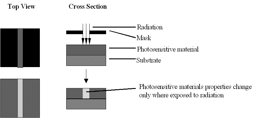
Figure 1: Transfer of a pattern to a photosensitive material.
This discussion will focus on optical lithography, which is simply lithography using a radiation source with wavelength(s) in the visible spectrum.
In lithography for micromachining, the photosensitive material used is typically a photoresist (also called resist, other photosensitive polymers are also used). When resist is exposed to a radiation source of a specific a wavelength, the chemical resistance of the resist to developer solution changes. If the resist is placed in a developer solution after selective exposure to a light source, it will etch away one of the two regions (exposed or unexposed). If the exposed material is etched away by the developer and the unexposed region is resilient, the material is considered to be a positive resist (shown in figure 2a). If the exposed material is resilient to the developer and the unexposed region is etched away, it is considered to be a negative resist (shown in figure 2b).
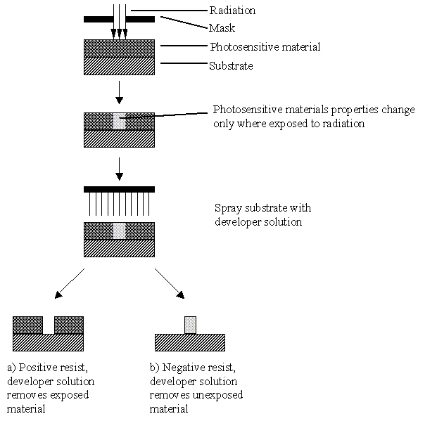
Figure 2: a) Pattern definition in positive resist, b) Pattern definition in negative resist.
Lithography is the principal mechanism for pattern definition in micromachining. Photosensitive compounds are primarily organic, and do not encompass the spectrum of materials properties of interest to micro-machinists. However, as the technique is capable of producing fine features in an economic fashion, a photosensitive layer is often used as a temporary mask when etching an underlying layer, so that the pattern may be transferred to the underlying layer (shown in figure 3a). Photoresist may also be used as a template for patterning material deposited after lithography (shown in figure 3b). The resist is subsequently etched away, and the material deposited on the resist is "lifted off".
The deposition template (lift-off) approach for transferring a pattern from resist to another layer is less common than using the resist pattern as an etch mask. The reason for this is that resist is incompatible with most MEMS deposition processes, usually because it cannot withstand high temperatures and may act as a source of contamination.
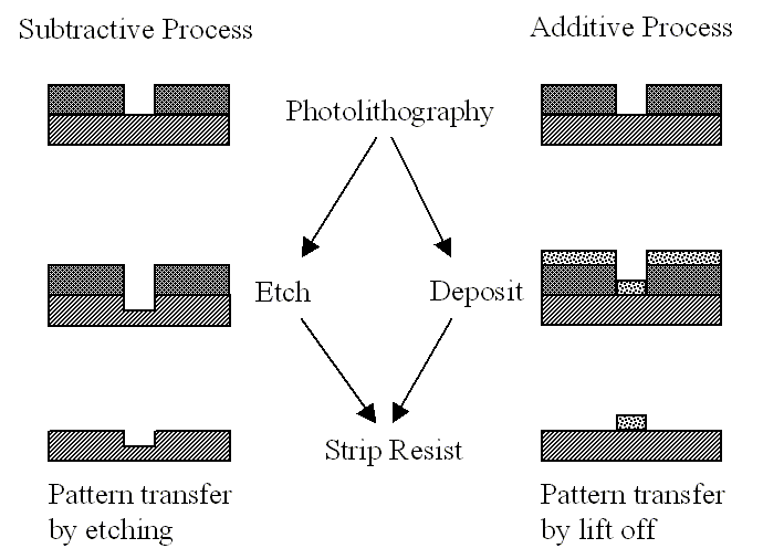
Figure 3:
a) Pattern transfer from patterned photoresist to underlying layer by
etching
b) Pattern transfer from patterned photoresist to overlying
layer by lift-off
Once the pattern has been transferred to another layer, the resist is usually stripped. This is often necessary as the resist may be incompatible with further micromachining steps. It also makes the topography more dramatic, which may hamper further lithography steps.
In order to make useful devices the patterns for different lithography steps that belong to a single structure must be aligned to one another. The first pattern transferred to a wafer usually includes a set of alignment marks, which are high precision features that are used as the reference when positioning subsequent patterns, to the first pattern (as shown in figure 4). Often alignment marks are included in other patterns, as the original alignment marks may be obliterated as processing progresses. It is important for each alignment mark on the wafer to be labeled so it may be identified, and for each pattern to specify the alignment mark (and the location thereof) to which it should be aligned. By providing the location of the alignment mark it is easy for the operator to locate the correct feature in a short time. Each pattern layer should have an alignment feature so that it may be registered to the rest of the layers.
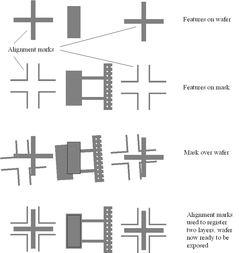
Figure 4: Use of alignment marks to register subsequent layers
Depending on the lithography equipment used, the feature on the mask used for registration of the mask may be transferred to the wafer (as shown in figure 5). In this case, it may be important to locate the alignment marks such that they don't effect subsequent wafer processing or device performance. For example, the alignment mark shown in figure 6 will cease to exist after a through the wafer DRIE etch. Pattern transfer of the mask alignment features to the wafer may obliterate the alignment features on the wafer. In this case the alignment marks should be designed to minimize this effect, or alternately there should be multiple copies of the alignment marks on the wafer, so there will be alignment marks remaining for other masks to be registered to.
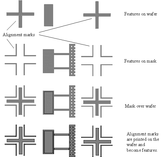
Figure 5: Transfer of mask registration feature to substrate during lithography (contact aligner)
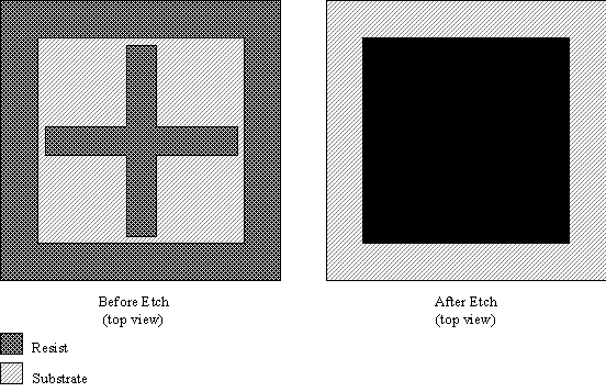
Figure 6:
Poor alignment mark design for a DRIE through the wafer etch
(cross hair is released and lost).
Alignment marks may not necessarily be arbitrarily located on the wafer, as the equipment used to perform alignment may have limited travel and therefore only be able to align to features located within a certain region on the wafer (as shown in figure 7). The region location geometry and size may also vary with the type of alignment, so the lithographic equipment and type of alignment to be used should be considered before locating alignment marks. Typically two alignment marks are used to align the mask and wafer, one alignment mark is sufficient to align the mask and wafer in x and y, but it requires two marks (preferably spaced far apart) to correct for fine offset in rotation.
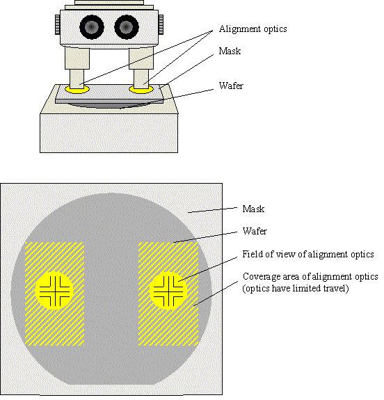
Figure 7: Restriction of location of alignment marks based on equipment used.
As there is no pattern on the wafer for the first pattern to align to, the first pattern is typically aligned to the primary wafer flat (as shown in figure 8). Depending on the lithography equipment used, this may be done automatically, or by manual alignment to an explicit wafer registration feature on the mask.
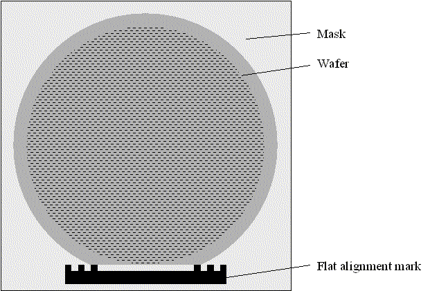
Figure 8: Mask alignment to the wafer flat.
The exposure parameters required in order to achieve accurate pattern transfer from the mask to the photosensitive layer depend primarily on the wavelength of the radiation source and the dose required to achieve the desired properties change of the photoresist. Different photoresists exhibit different sensitivities to different wavelengths. The dose required per unit volume of photoresist for good pattern transfer is somewhat constant; however, the physics of the exposure process may affect the dose actually received. For example a highly reflective layer under the photoresist may result in the material experiencing a higher dose than if the underlying layer is absorptive, as the photoresist is exposed both by the incident radiation as well as the reflected radiation. The dose will also vary with resist thickness.
There are also higher order effects, such as interference patterns in thick resist films on reflective substrates, which may affect the pattern transfer quality and sidewall properties.
At the edges of pattern light is scattered and diffracted, so if an image is overexposed, the dose received by photoresist at the edge that shouldn't be exposed may become significant. If we are using positive photoresist, this will result in the photoresist image being eroded along the edges, resulting in a decrease in feature size and a loss of sharpness or corners (as shown in figure 9). If we are using a negative resist, the photoresist image is dilated, causing the features to be larger than desired, again accompanied by a loss of sharpness of corners. If an image is severely underexposed, the pattern may not be transferred at all, and in less sever cases the results will be similar to those for overexposure with the results reversed for the different polarities of resist.
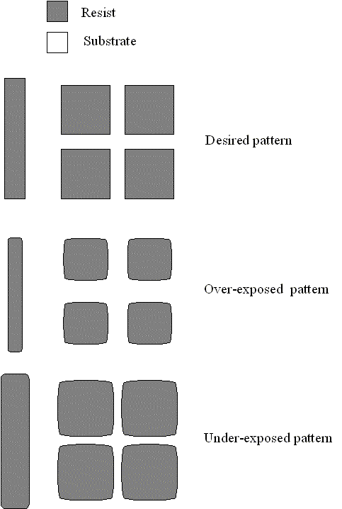
Figure 9: Over and under-exposure of positive resist.
If the surface being exposed is not flat, the high-resolution image of the mask on the wafer may be distorted by the loss of focus of the image across the varying topography. This is one of the limiting factors of MEMS lithography when high aspect ratio features are present. High aspect ratio features also experience problems with obtaining even resist thickness coating, which further degrades pattern transfer and complicates the associated processing.
Typically lithography is performed as part of a well-characterized module, which includes the wafer surface preparation, photoresist deposition, alignment of the mask and wafer, exposure, develop and appropriate resist conditioning. The lithography process steps need to be characterized as a sequence in order to ensure that the remaining resist at the end of the modules is an optimal image of the mask, and has the desired sidewall profile.
The standard steps found in a lithography module are (in sequence): dehydration bake, HMDS prime, resist spin/spray, soft bake, alignment, exposure, post exposure bake, develop hard bake and descum. Not all lithography modules will contain all the process steps. A brief explanation of the process steps is included for completeness.
We make a few assumptions about photolithography. Firstly, we assume that a well characterized module exists that: prepares the wafer surface, deposits the requisite resist thickness, aligns the mask perfectly, exposes the wafer with the optimal dosage, develops the resist under the optimal conditions, and bakes the resist for the appropriate times at the appropriate locations in the sequence. Unfortunately, even if the module is executed perfectly, the properties of lithography are very feature and topography dependent. It is therefore necessary for the designer to be aware of certain limitations of lithography, as well as the information they should provide to the technician performing the lithography.
The designer influences the lithographic process through their selections of materials, topography and geometry. The material(s) upon which the resist is to be deposited is important, as it affects the resist adhesion. The reflectivity and roughness of the layer beneath the photoresist determines the amount of reflected and dispersed light present during exposure. It is difficult to obtain a nice uniform resist coat across a surface with high topography, which complicates exposure and development as the resist has different thickness in different locations. If the surface of the wafer has many different height features, the limited depth of focus of most lithographic exposure tools will become an issue (as shown in figure 10).
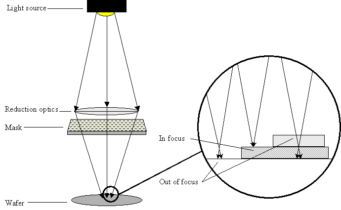
Figure 10: Lithography tool depth of focus and surface topology.
The designer should keep all these limitations in mind, and design accordingly. For example, it is judicious, when possible, to perform very high aspect patterning step (lithography and subsequent etch/deposition) last, as the topography generated often hampers any further lithography steps. It is also necessary for the designer to make it clear which focal plane is most important to them (keeping in mind that features further away in Z from the focal plane will experience the worst focus). The resolution test structures should be located at this level (as they will be used by the fab to check the quality of a photo step).