4. Introduction to Mask Making
Mask making consists of two steps, layout (defining the pattern that will appear on the mask) and pattern transfer to the mask. First we discuss the materials that comprise the mask.
4.1. Mask Materials
4.1.1. Mask substrates
For optical lithography, it is essential that the substrate used to make a mask be transparent to optical wavelengths and have extremely flat defect-free surfaces. It is preferable that the substrate have a coefficient of thermal expansion very similar to silicon. Commonly used substrates are soda-lime glass and quartz. Quartz masks have a very similar coefficient of thermal expansion to silicon, but are somewhat more expensive than soda-lime masks. Any temperature variation may have a significant effect on masks with a substrate with a high coefficient of thermal expansion (relative to the substrate), as a small change in the dimensions of the mask, may translate to a big change in the position of a fine feature on the mask.
4.1.2. Mask Coatings
For optical lithography it is necessary for the coating on the surface of the mask substrate (i.e. the material that will define the pattern on the mask) be opaque to optical wavelengths, and easily patterned with high definition. The patterning of the coating should not affect the substrate in such a manner that its properties as a mask substrate are degraded. The two most common mask coating materials used for optical lithography are emulsion and chrome. Emulsion is much cheaper to make; however, the coating is not of as high a quality as chrome, and doesn't last as well through the rigors of processing. There are also potential contamination issues with emulsion masks. Iron Oxide coatings are also used, but are less common than emulsion or chrome, the price and quality falls somewhere between the two. Some people favor semi-transparent chrome or iron oxide for contact aligners, as the layers are semi-transparent, which may aid alignment. Small features are not easily viewed through semi-transparent mask coatings, so one may still require large open windows in the mask to aid alignment.
4.2. Layout
Layout is the process of defining the patterns that will be transferred to your masks, and as such will define the geometry of your devices. Layout is typically performed in a graphical editing tool such as Ledit, Magic, KIC, Cadence etc. The layout tool manipulates a file that contains layers of patterns. Masks correspond to layers. In order to simplify registration of features on one mask to another, the layout tool usually allows the user to view and edit all the layer together, or selected layers. These tools support the generation of a series of basic shapes. The shapes may be grouped into cells, which in turn may be incorporated with other shapes and cells into hierarchies of cells (as shown in figure 18). Cells may include shapes from different levels in the layout. It is important to remember and convey the name of the root cell for your layout (i.e. the top level cell) to ensure that all the features intended appears in a mask (as opposed to lower level cell).
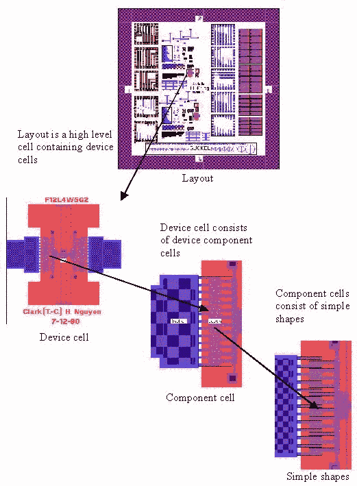
Fig. 18. Hierarchical nature of layout tools
It is important to use distinct layer names for each layer in the layout, and to remember what the layer designation is for each layer (layer designator type varies depending on the layout file format). This is necessary for mask making, to ensure that each layer may be located and referred to. It may also be useful during layout to define symbolic layers (not intended to be made into masks). Symbolic layers must be labeled as such, to ensure that they don't get made into masks.
Some high end tools allow the mask set to be compiled with a process sequence to generate three dimensional renderings of the expected devices. Once all the features in all the layers have been entered, and the user has included the appropriate alignment features, the layout is ready for submission.
For some layers it is easier to do the layout for the reverse polarity image of the features (as shown in figure 19). The polarity of the layer is simply reversed during the mask making process. The polarity of the mask must be indicated by either brightfield (space left open in layout is transparent, also known as clearfield or lightfield) or darkfield (space left open in layout is opaque). Note that you may also require a polarity reversal depending on the type of resist you are using, and the method of pattern transfer (additive or subtractive).
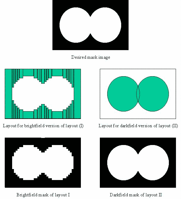
Fig. 19. Layout of reverse polarity images
4.3. Pattern Transfer
Mask substrates are purchased already coated with the necessary mask coating, and are typically patterned using photolithography and a subsequent etch. The patterning of the resist is commonly done in three ways: ruby lithography, pattern generation and e-beam.
4.3.1. Ruby Lithography
Ruby lithography is a technique of printing, in which a pattern is made from a thin layer of filter plastic, which may then be used as a mask to transfer the pattern to a photosensitive material. In order to make a mask for semiconductor processing using ruby lithography, an enlarged plot of the mask image is made on the filter plastic using a sharp blade. The pattern produced in the plastic layer is then reduction printed to transfer the pattern to a mask. The resolution is limited both by the printing reduction optics and smallest feature that can be safely cut from the plastic. This technique is seldom used any more.
4.3.2 Pattern Generation
Pattern generation involves the use of a rectangular shutter which is capable of variable size and orientation. The shutter is used to sequentially expose the resist on the mask substrate until the requisite pattern is fully defined. Typically the smallest size the shutter is capable of is a 2um square. The pattern to be transferred has to be segmented into the smallest number of boxes possible, and then the mask is sequentially exposed box by box until the entire pattern has been transferred. As the mask is exposed sequentially, small intricate features and curved features may require a large number of flashes to define the pattern. A pattern with a high flash count may make this method of mask pattern transfer uneconomic.
4.3.3 E-beam
E-beam is a technique, in which an electron beam is used to selectively expose the resist on the mask. The beam is raster scanned across the wafer, defining the pattern. The beam may be made very narrow, so that very intricate features may be defined using this approach. The time to scan an entire mask is approximately constant for a specific beam width and pattern area, so regardless of the complexity of the layout, the cost is the similar for a specific beam width and write area. For layouts including smooth curves and many off scan orientation lines, a narrow beam must be used to achieve smooth edges. The narrower the beam used, the longer the write time for a mask (as more scans are required), which increases the cost.